德拉姆

DRAM缩放需要新材料工程解决方案

计算的AI时代正在助长数据生成的指数增长,整个技术生态系统取决于半导体行业,找到了扩展DRAM体系结构的新方法,以使步伐保持需求。新的硬面膜图案薄膜可以使具有最高纵横比的较薄的电容器,而新的电介质绝缘材料可以减少金属线之间的间距,这两者都产生了新的收缩方式。
新回忆是中心舞台

新回忆是中心舞台

就像厄运的各种先知预言摩尔定律的灭亡一样,我们经常听到传统的记忆技术很快就会消失。但是,半导体行业高度技巧,可以扩展其现有架构,而不是迈向具有明显令人信服的优势的闪亮新架构。因此,传统技术的增量进步推迟了引入一系列令人兴奋的新记忆技术。什么时候到达临界点,将一个或多个推入主流?阅读企业中一些最知识的思想在跳跃之后必须说的话。
亚博最新版本

总回忆:高级性能和功率效率的高级记忆技术

由于更快,更强大的智能手机,平板电脑和笔记本电脑,移动计算现在都比以往任何时候都更加多。are going to keep up with consumers’ constant demand for higher performance, longer battery life and ultra-sleek profiles.To address these technology improvements and answer key questions that may significantly impact the way we interface with an increasingly connected world, Applied Ventures and the MIT Club of Northern California (MITCNC) will host a lively panel discussion with innovators from across the memory value chain on Wednesday, February 1 at 6:30pm in Santa Clara, Calif.[edit: you can read a report from the session here.]
3D芯片技术用于假人

3D芯片技术用于假人

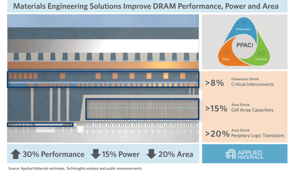
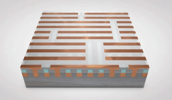
It's not just movies, televisions and video games that are going three-dimensional these days. Microchips are doing it, too.Semiconductors aren't shifting into the third dimension because it’s fashionable, though. This shift is about continuing Moore’s Law, the relentless drive for higher performance that has driven the industry for four decades.With three very different types of 3D construction in development today, it can be a confusing subject. Vertical chip structures, 3D device stacking, 3D chip packaging – what does it all mean?We made this video to help demystify the subject. Did it help? Let me know in the comments below.